SKU: SBCD-0560
📋 GST Invoice Available

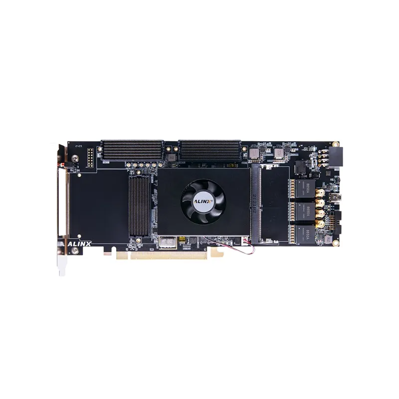
Alinx AXVU13P Virtex US+ XCVU13P FPGA Dev Board

₹2,065,499.00 (Inclusive of all taxes)
Out of Stock

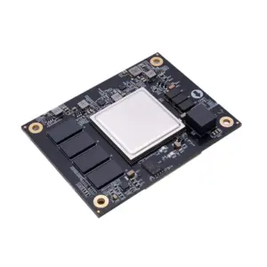
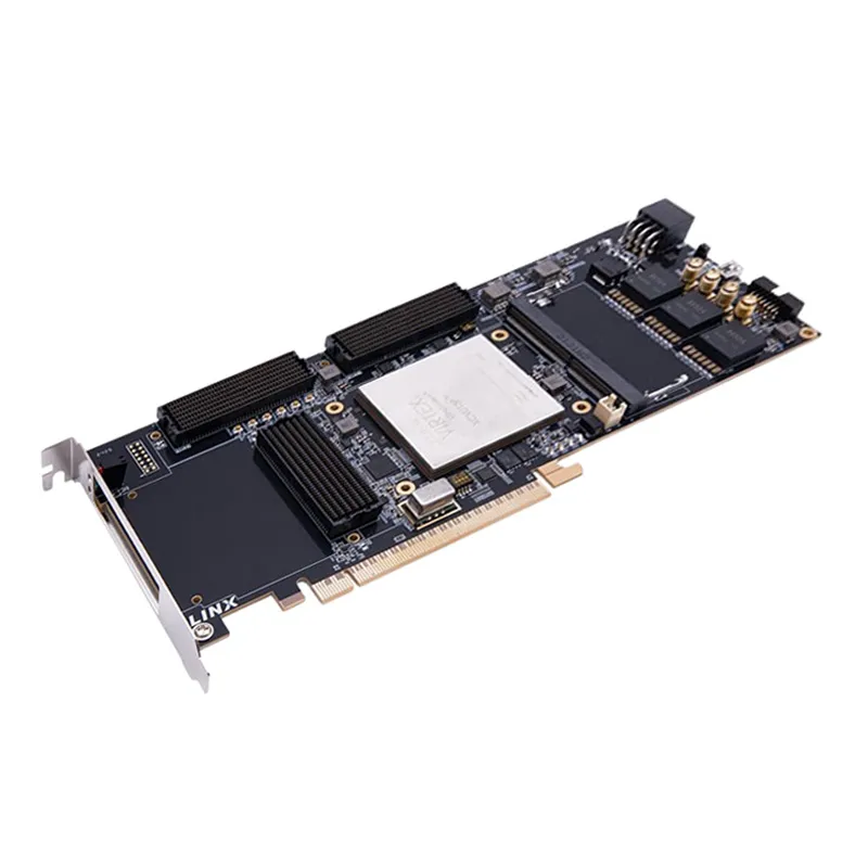
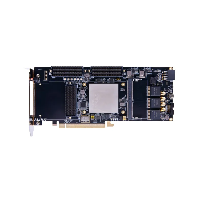
The Alinx AXVU13P is a high-performance FPGA development board featuring the AMD/Xilinx Virtex UltraScale+ XCVU13P, designed for demanding applications in AI/ML, network acceleration, and compute acceleration. It offers extensive expansion via three FMC+ connectors and robust high-speed I/O.

Features

  • Powered by AMD/Xilinx Virtex UltraScale+ XCVU13P-2FHGB2104I FPGA.
  • Supports up to 16GB DDR4 SODIMM and 256MB QSPI Flash memory.
  • Features PCIe Gen3 x16, integrated 100G Ethernet MAC, and 150G Interlaken cores.
  • Equipped with three versatile FMC+ connectors for extensive I/O expansion.
  • Delivers up to 38 TOPs DSP performance, optimized for AI/ML inference and compute acceleration.

Out of stock

Description

The Alinx AXVU13P FPGA development board is engineered around the formidable AMD/Xilinx Virtex UltraScale+ XCVU13P-2FHGB2104I, providing an advanced platform for highly demanding, high-speed digital processing applications. This board distinguishes itself with exceptional flexibility, featuring three high-bandwidth FMC+ connectors that enable seamless integration with a diverse array of expansion modules. This makes it an ideal choice for complex use cases spanning machine learning, artificial intelligence, cutting-edge network acceleration, and 5G baseband processing.

Equipped with an integrated 100G Ethernet MAC, a high-throughput PCIe Gen3 x16 interface, and an impressive 38 TOPs of DSP compute performance, the AXVU13P excels in areas such as compute acceleration, radar systems, and hardware emulation. Its substantial DDR4 memory slot supporting up to 16GB, along with integrated QSPI flash and extensive transceiver support, ensures it is well-suited for mission-critical tasks in fields like wired communications development and high-fidelity prototyping.

Key Features

  • Powered by the AMD/Xilinx Virtex UltraScale+ XCVU13P-2FHGB2104I FPGA with 16nm FinFET architecture.
  • Offers massive compute capability with up to 38 TOPs (Tera Operations Per Second) for AI inference.
  • Integrates high-speed communication interfaces including PCIe Gen3 x16, 100G Ethernet MAC, and 150G Interlaken cores.
  • Provides advanced connectivity through three FMC+ connectors: FMC+1 (120 IOs + 20 GTY), FMC+2 (120 IOs + 16 GTY), FMC+3 (164 IOs + 24 GTY).
  • Supports high-speed memory with one DDR4 SODIMM slot (up to 16GB) and two 128MB QSPI Flash modules (total 256MB).
  • Includes rich I/O and debug interfaces: 2x SMA, 1x UART (USB to UART), 1x JTAG header, 8x User LEDs, and 1x Push Button.
  • Designed for efficiency with a single 12V power supply.

Applications

  • High-performance AI/Machine Learning inference and acceleration.
  • Network acceleration and high-speed data processing (e.g., 100G Ethernet, 150G Interlaken).
  • 5G baseband processing and telecommunications infrastructure.
  • Compute acceleration for demanding scientific and engineering tasks.
  • Radar and signal processing systems.
  • Hardware emulation and prototyping of complex digital designs.
  • Advanced wired communications development.

Technical Specifications

FPGA DeviceAMD/Xilinx Virtex UltraScale+ XCVU13P-2FHGB2104I
Architecture16nm FinFET
DSP PerformanceUp to 38 TOPs (Tera Operations Per Second)
Memory1x DDR4 SODIMM slot (up to 16GB), 2x 128MB QSPI Flash (256MB total)
PCIe InterfacePCIe Gen3 x16
Ethernet100G Ethernet MAC
InterlakenSupports 150G Interlaken cores
Expansion Connectors3x FMC+ (FMC+1: 120 IOs + 20 GTY, FMC+2: 120 IOs + 16 GTY, FMC+3: 164 IOs + 24 GTY)
I/O & Debug2x SMA, 1x UART (USB to UART), 1x JTAG, 8x User LEDs, 1x Push Button
Power Supply12V single supply
Board Dimensions251mm x 111.15mm

Frequently Asked Questions

What is the primary FPGA on the Alinx AXVU13P board?

The board features the AMD/Xilinx Virtex UltraScale+ XCVU13P-2FHGB2104I FPGA. This high-end device, built on a 16nm FinFET process, is designed for extreme performance in data centers, high-speed networking, and advanced compute acceleration tasks, offering massive logic and DSP resources for complex designs.

What expansion options does the AXVU13P offer for custom peripherals?

The AXVU13P provides extensive expansion through three FMC+ (FPGA Mezzanine Card+) connectors. These connectors support a high number of single-ended and differential I/O lines, along with multiple GTY transceivers, enabling integration with a wide range of high-bandwidth daughter cards and custom modules for specific application requirements.

What kind of performance can be expected for AI/ML applications?

This board is highly optimized for AI/ML inference, capable of delivering up to 38 TOPs (Tera Operations Per Second) of DSP performance. The Virtex UltraScale+ architecture efficiently handles fixed-point and floating-point arithmetic, making it suitable for accelerating deep learning models and other compute-intensive algorithms at the edge or in data centers.

What memory interfaces are available on the Alinx AXVU13P?

The AXVU13P includes a SODIMM slot for up to 16GB of high-speed DDR4 memory, providing substantial bandwidth for large datasets and complex algorithms. Additionally, it features two 128MB QSPI Flash modules, totaling 256MB, which are essential for storing FPGA bitstreams, configuration data, and system boot images.

What are the primary communication interfaces supported by the board?

The board boasts robust communication interfaces, including a PCIe Gen3 x16 slot for high-throughput host connectivity and an integrated 100G Ethernet MAC for high-speed networking. It also supports 150G Interlaken cores, facilitating very high-bandwidth chip-to-chip or board-to-board communication for network processing units.

Package Includes

  • 1x Alinx AXVU13P FPGA Development Board with AMD Virtex UltraScale+ XCVU13P

Additional Information

Weight 1.6 kg
Dimensions 25.1 × 11.115 cm