SKU: IOWC-1042
📋 GST Invoice Available

EP4CE6E22 FPGA Core Development Board (Cyclone IV)

₹1,279.00 (Inclusive of all taxes)
Out of Stock

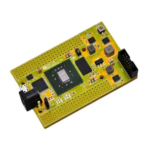
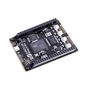
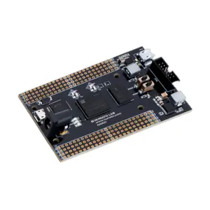
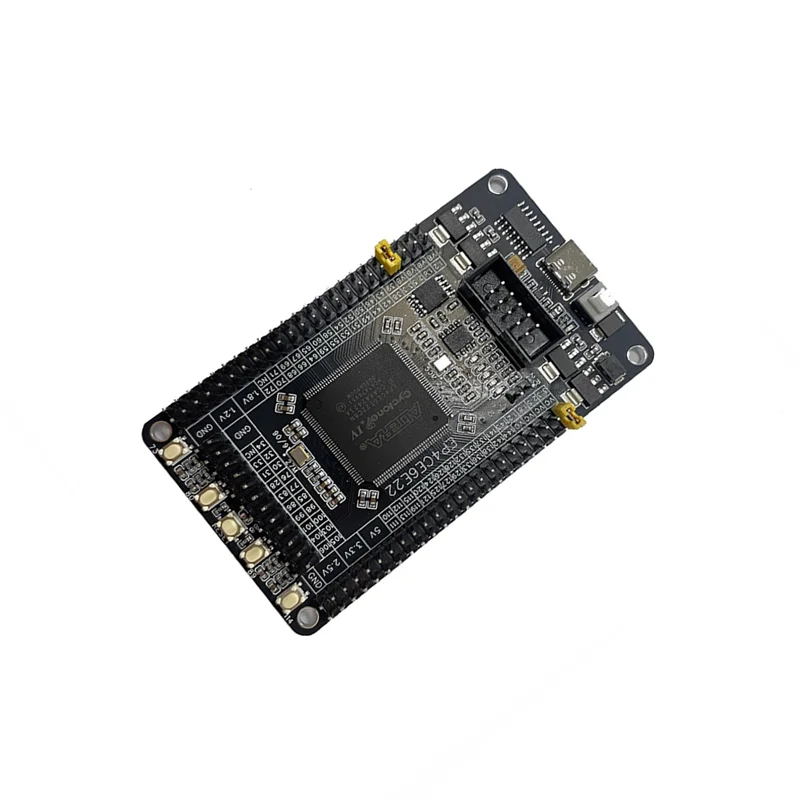
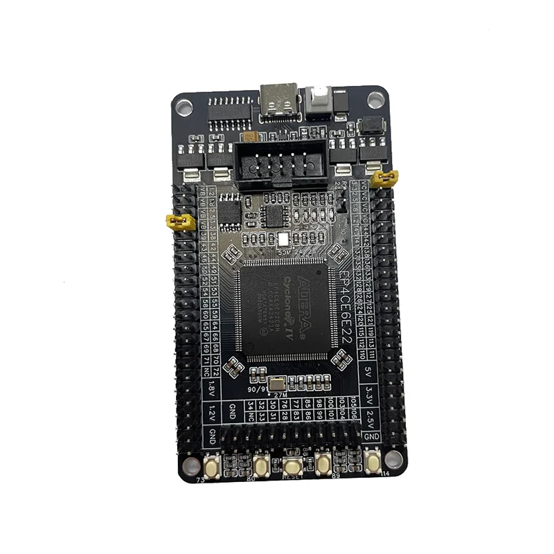
The EP4CE6E22 FPGA Core Development Board is a compact digital design platform centered on the Altera Cyclone IV EP4CE6E22 FPGA, featuring a CH340 USB-to-UART interface, configurable I/O voltage levels, and onboard SPI flash for firmware storage, ideal for prototyping and embedded systems education.

Features

  • Cyclone IV EP4CE6E22 FPGA provides a robust, low-cost platform for digital logic design, signal processing, and custom peripheral implementation.
  • Configurable I/O voltage (1.2V to 5V) via jumper caps ensures seamless interfacing with a wide range of sensors, displays, and communication modules.
  • Onboard CH340 USB-to-Serial chip and W25Q SPI Flash simplify programming, debugging, and non-volatile firmware storage.
  • Dual 50MHz & 27MHz crystal oscillators offer flexible clocking options for timing-critical applications and peripheral synchronization.
  • Five user LEDs and five pull-up pushbuttons provide immediate feedback and input for rapid prototyping and hardware testing.

Out of stock

Description

The EP4CE6E22 FPGA Development Board is engineered for digital design exploration and embedded systems development. Its core is the Altera Cyclone IV EP4CE6E22 FPGA, offering a balance of logic elements and power efficiency for implementing custom processors, state machines, and hardware accelerators. The board integrates essential peripherals, including a CH340 USB-to-UART bridge for serial communication and a W25Q SPI flash chip for persistent configuration storage, streamlining the development workflow.

Power management is a key feature, with user-selectable I/O voltage levels from 1.2V to 5V, allowing direct connection to 3.3V microcontrollers, 5V legacy systems, or low-voltage sensors without external level shifters. The dual onboard oscillators provide stable clock sources for the FPGA core and external interfaces. With dedicated JTAG headers for programming via a USB Blaster and a USB Type-C port for power and data, the board offers a complete, self-contained environment for FPGA-based IoT and hardware prototyping projects.

Key Features

  • Core FPGA platform based on Altera Cyclone IV EP4CE6E22 for custom digital logic implementation.
  • Flexible I/O voltage configuration (1.2V, 1.8V, 2.5V, 3.3V, 5V) via jumper caps for universal module compatibility.
  • Integrated CH340 USB-to-Serial converter provides reliable UART communication for debugging and data transfer.
  • Onboard W25Q SPI Flash memory stores FPGA configuration bitstreams or application data persistently.
  • Dual crystal oscillators (50 MHz and 27 MHz) supply precise clock signals for core and peripheral timing.
  • Five user-controllable LEDs and five tactile pushbuttons enable immediate hardware interaction and input testing.
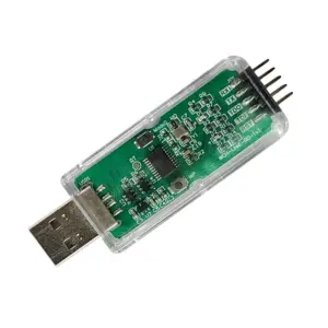
  • Standard 10-pin JTAG header supports programming and debugging with Altera USB Blaster or compatible tools.
  • Compact form factor powered via USB Type-C, making it portable and easy to integrate into test setups.

Applications

  • Digital logic and computer architecture education for university courses and self-learning.
  • Prototyping custom digital circuits, state machines, and hardware accelerators for embedded systems.
  • Developing interface bridges and protocol converters (e.g., SPI to I2C, custom serial communication).
  • Implementing real-time signal processing algorithms for audio, video, or sensor data.
  • Creating hardware test fixtures and validation platforms for electronic component testing.

Technical Specifications

FPGAAltera Cyclone IV EP4CE6E22
USB InterfaceCH340 (USB-to-UART)
Flash StorageW25Q SPI Flash
Clock Sources50 MHz & 27 MHz onboard crystals
User I/O5 LEDs, 5 pushbuttons
I/O Voltage RangeConfigurable 1.2V, 1.8V, 2.5V, 3.3V, 5V
Fixed Voltage PinsRight-side pins fixed at 3.3V
Programming InterfaceJTAG (10-pin header)
Power InputUSB Type-C
Dimensions89 mm (L) x 36 mm (W)
Weight29 g

Frequently Asked Questions

How do I program the EP4CE6E22 FPGA on this development board?

You program the FPGA using Altera Quartus Prime software. Connect a USB Blaster cable to the board's 10-pin JTAG header. In Quartus, compile your Verilog or VHDL design into a .sof file, then use the Programmer tool to download it via JTAG. For persistent storage, you can configure the W25Q SPI flash to load the bitstream on power-up. The CH340 provides a separate UART interface for serial communication with your FPGA design after programming.

How do I configure the I/O pin voltage levels on this board?

The board has jumper caps near the I/O pin headers labeled for voltage selection (e.g., 1.2V, 3.3V, 5V). Place a jumper cap on the two pins corresponding to your desired logic level for that I/O bank. Ensure the connected peripheral modules operate at the same voltage to prevent damage. Note that a group of pins on the right side is fixed at 3.3V and is not configurable. Always power off the board before changing jumper settings.

What is the purpose of the dual onboard oscillators (50MHz & 27MHz)?

The 50 MHz oscillator typically serves as the primary clock for the FPGA's internal logic and PLLs, enabling high-speed operations. The 27 MHz clock is often used as a reference for video or audio applications, such as VGA signal generation or audio sampling, where standard timings are required. You can select which oscillator to use globally or for specific modules within your FPGA design via the Quartus Pin Planner and clock management IP cores.

Can I use the onboard W25Q SPI Flash to store data from my FPGA design?

Yes, the W25Q flash is connected to the FPGA via SPI pins and can store both the FPGA configuration bitstream and application data. To store user data, you must instantiate an SPI controller in your FPGA design to communicate with the flash, handling commands for reading, writing, and erasing sectors. The CH340 UART can relay data between a PC and the FPGA, which can then be written to the flash. Ensure your design manages the flash's busy status and wear-leveling for robust operation.

Package Includes

  • 1 x EP4CE6E22-FPGA Core Development Board

Additional Information

Weight 0.029 kg
Dimensions 8.9 × 3.6 cm