SKU: IOWC-1290
📋 GST Invoice Available

Sipeed Tang Nano 1K FPGA Development Board (GW1NZ-LV1)

₹979.00 (Inclusive of all taxes)
Out of Stock

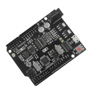
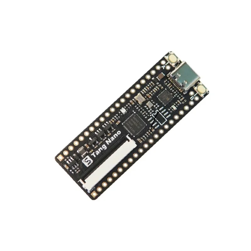
The Sipeed Tang Nano 1K is a compact FPGA development board centered on the Gowin GW1NZ-LV1 chip, designed for digital logic design, embedded system prototyping, and educational projects with its integrated USB-JTAG debugger and RGB LCD interface.

Features

  • Features the Gowin GW1NZ-LV1 FPGA with 1152 LUT4 logic units and 64Kb block SRAM for small-scale digital designs.
  • Integrated USB-JTAG debugger simplifies programming and in-circuit debugging without external hardware.
  • Onboard FPC connector and circuit for direct interfacing with RGB LCD displays and other peripherals.
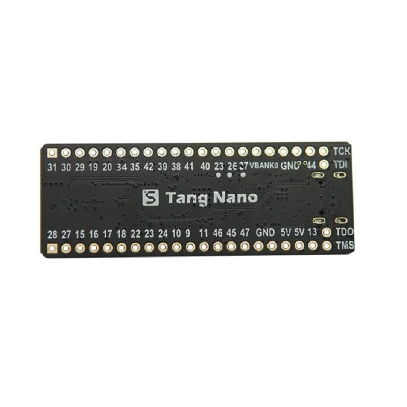
  • Provides 44 user I/O pins across 4 banks for flexible external device connectivity and expansion.
  • Compact form factor (58.34 x 21.29mm) with programmable RGB LED and two user buttons for rapid prototyping.

Out of stock

Description

The Sipeed Tang Nano 1K is a dedicated development platform for the Gowin GW1NZ-LV1 FPGA, offering a complete solution for experimenting with hardware description languages (HDLs) and digital logic. Its core provides 1152 Lut4 logic units, 864 registers, and 72K bits of block SRAM, supported by 128Kb of user flash memory for non-volatile configuration storage. The board’s architecture includes two Phase-Locked Loops (PLLs) for clock management and four I/O banks, enabling stable signal generation and flexible pin assignment.

Designed for ease of integration, the Tang Nano 1K includes an onboard USB-JTAG interface that streamlines the firmware upload and debugging workflow, eliminating the need for external programmers. The inclusion of a WSON8 pad and a dedicated FPC connector facilitates advanced projects involving external memory or display modules. With an operating temperature range of -10°C to 65°C and a minimal power profile, this board is suitable for both educational environments and proof-of-concept development in embedded vision and control systems.

Key Features

  • Core FPGA module based on the Gowin GW1NZ-LV1 chip with 1152 Lut4 logic units and 864 flip-flops.
  • Integrated USB-JTAG debugger provides seamless programming and real-time hardware debugging capabilities.
  • Onboard FPC connector and supporting circuitry for direct attachment of RGB LCD screens and other flat-panel displays.
  • Dedicated WSON8 footprint allows for soldering additional serial flash memory for expanded storage.
  • Features two user-programmable tactile buttons and one programmable RGB LED for interactive feedback and control.
  • Equipped with 44 user-accessible I/O pins organized into 4 banks, supporting 3.3V LVCMOS logic levels.
  • Compact and lightweight design ideal for portable embedded applications and integration into final assemblies.

Applications

  • Educational platform for learning FPGA design, Verilog, and VHDL.
  • Prototyping custom digital logic circuits, state machines, and accelerators.
  • Driving RGB LCD displays and creating simple graphical interfaces.
  • Developing hardware for embedded control systems and IoT sensor fusion.
  • Implementing lightweight cryptographic algorithms and signal processing blocks.

Technical Specifications

FPGA ChipGowin GW1NZ-LV1
Logic Units (LUT4)1152
Registers (FF)864
Block SRAM72K bits
User Flash128K bits
PLLs2
I/O Banks4
User I/O Pins44
Onboard InterfacesUSB-JTAG, FPC Connector, WSON8 Pad
User Inputs/Outputs2 Programmable Buttons, 1 Programmable RGB LED
Operating Temperature-10°C to +65°C
Board Dimensions58.34mm (L) x 21.29mm (W)

Frequently Asked Questions

What software toolchain is required to program the Tang Nano 1K FPGA?

You need to install Gowin's official FPGA design software, Gowin EDA, which includes synthesis, place-and-route, and programming tools. After writing your design in Verilog or VHDL within the IDE, you generate a bitstream file. Connect the board via its onboard USB port, and use the software's programmer utility to flash the bitstream directly through the integrated USB-JTAG interface, configuring the FPGA's logic.

How do I connect an LCD display to the Tang Nano 1K board?

The board features a dedicated FPC (Flexible Printed Circuit) connector. You will need a compatible RGB LCD module with a matching FPC cable. Connect it directly to the onboard connector. Then, in your FPGA design, you must implement the appropriate display controller IP or write HDL code to drive the LCD's RGB data, sync, and clock signals using the I/O pins routed to that connector, referencing the board's pinout diagram.

Can I use the onboard WSON8 pad to add more memory?

Yes, the WSON8 pad is designed for attaching an external serial Flash memory chip, such as a 25-series SPI Flash. You would need to solder a compatible WSON8 package chip onto the pads. In your FPGA design, you must then instantiate a SPI controller IP core or write HDL to communicate with this external memory, allowing you to store additional configuration data, firmware, or application assets beyond the internal 128Kb flash.

What is the purpose of the two programmable buttons and RGB LED?

The two tactile buttons are connected to general-purpose I/O pins of the FPGA, allowing you to define them as inputs for user control, reset signals, or mode selection in your design. The RGB LED is also connected to FPGA pins; you can implement a PWM controller in your HDL code to drive its red, green, and blue channels independently, creating status indicators, debugging visual outputs, or dynamic lighting effects for your project.

Package Includes

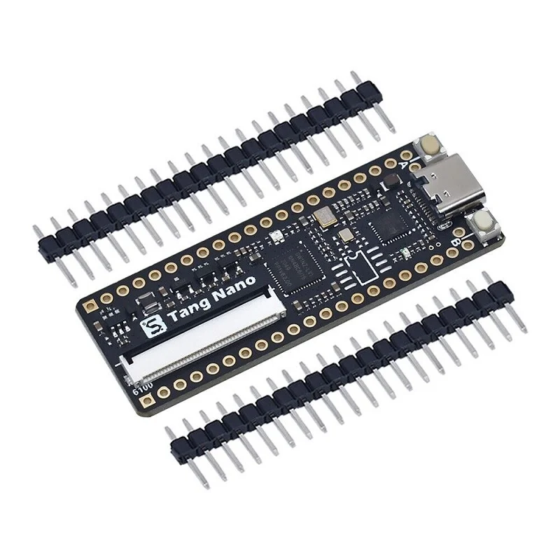
  • 1 x Sipeed Tang Nano 1K Core Board
  • 2 x 22-Pin 2.54mm Male Headers

Additional Information

Weight 0.01 kg
Dimensions 5.834 × 2.129 cm