SKU: SBCD-0573
📋 GST Invoice Available

Lattice ECP5-5G LFE5UM5G-85F FPGA Evaluation Board

₹14,869.00 (Inclusive of all taxes)
Out of Stock

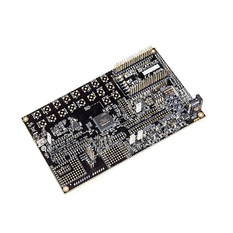
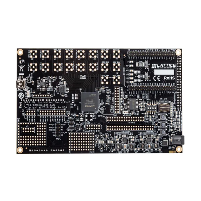
The Lattice ECP5-5G Evaluation Board (LFE5UM5G-85F-EVN) provides a robust platform for investigating and prototyping designs with the ECP5-5G Field Programmable Gate Array. It features essential peripherals like 128 Mbit SPI Flash, USB-B for programming, and various I/O for rapid development.

Features

  • Features the high-performance ECP5-5G FPGA (LFE5UM5G-85F-8BG381) for advanced logic designs.
  • Integrated USB-B connection simplifies device programming and I2C utility, supporting improved I3C.
  • Includes 128 Mbit SPI Flash with Quad read support for flexible boot and data storage.
  • On-board user interfaces such as 8 DIP switches, 3 push buttons, and 8 LEDs for demonstration and interaction.
  • Provides multiple reference clock sources to facilitate diverse application development.

Out of stock

Description

The Lattice ECP5-5G LFE5UM5G-85F-EVN Evaluation Board is engineered to empower designers and engineers in exploring the full capabilities of the ECP5-5G Field Programmable Gate Array. This board serves as an ideal environment for rapid prototyping, enabling efficient design investigation and verification of complex embedded systems. Its comprehensive feature set allows for thorough experimentation with logic implementations, high-speed interfaces, and custom digital circuits.

Equipped with a robust ECP5-5G FPGA, this evaluation board facilitates the development of demanding applications across various industries, including industrial control, telecommunications, and high-performance computing. The inclusion of essential peripherals like a 128 Mbit SPI Boot Flash and multiple reference clock sources ensures developers have the necessary tools for complex system integration. Its user-friendly programming interface and on-board debug resources streamline the development workflow from initial concept to final validation.

Key Features

  • Utilizes the ECP5-5G FPGA (LFE5UM5G-85F-8BG381) with advanced processing capabilities.
  • USB-B interface for seamless device programming, configuration, and I2C utility communication.
  • On-board 128 Mbit Serial Peripheral Interface (SPI) Flash memory with Quad read support for efficient boot and data storage.
  • Interactive user I/O including 8 DIP switches, 3 push buttons, and 8 LEDs for rapid prototyping and debugging.
  • Multiple configurable reference clock sources to support diverse timing requirements for complex designs.
  • Designed for rapid prototyping and testing of ECP5-5G FPGA-based specific hardware designs.

Applications

  • FPGA-based embedded system development and validation.
  • Rapid prototyping for custom logic and digital circuit designs.
  • High-speed data processing and communication applications.
  • Industrial control systems and automation.
  • Educational and research platforms for FPGA architectures.

Technical Specifications

FPGALattice ECP5-5G (LFE5UM5G-85F-8BG381)
Boot Flash Memory128 Mbit SPI Flash (Quad Read Support)
Programming/Utility InterfaceUSB-B (I2C utility, future I3C support)
User I/O8x DIP switches, 3x Push Buttons, 8x LEDs
Clock SourcesMultiple reference clock sources

Frequently Asked Questions

What is the primary purpose of the Lattice ECP5-5G Evaluation Board?

This board serves as a comprehensive platform for engineers to thoroughly investigate and rapidly prototype designs utilizing the ECP5-5G Field Programmable Gate Array. It enables hands-on experimentation with the FPGA's features, high-speed interfaces, and custom logic implementations for various embedded applications.

How is the ECP5-5G FPGA programmed on this evaluation board?

The ECP5-5G FPGA on the evaluation board is programmed via a USB-B connection. This interface not only handles device programming but also provides I2C utility, with future compatibility for improved I3C. This streamlined connectivity simplifies the configuration and debugging processes.

What type of on-board memory is available for the FPGA?

The evaluation board includes a 128 Mbit Serial Peripheral Interface (SPI) Boot Flash. This memory is crucial for storing the FPGA's configuration bitstream and application data. It also supports a Quad read feature, enhancing data access speed and overall system performance.

Can I use custom clock sources with this board?

Yes, the Lattice ECP5-5G Evaluation Board provides multiple reference clock sources. This flexibility allows designers to integrate and test custom clocking schemes for their specific applications, ensuring precise timing and synchronization for complex digital designs and high-speed interfaces.

Package Includes

  • 1 x Lattice Semiconductor LFE5UM5G-85F-EVN ECP5-5G FPGA Evaluation Board

Additional Information

Weight 0.775 kg
Dimensions 20 × 40 × 11 cm